![]()
SHANNON, CLARE, IRELAND, July 2, 2026 /EINPresswire.com/ — Announcing a new publication from Opto-Electronic Technology; DOI 10.29026/oet.2026.250014.
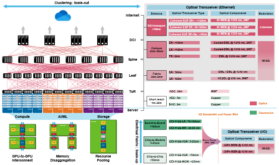
Driven by the rapid proliferation of Artificial Intelligence (AI) and High-Performance Computing (HPC), modern computing infrastructure faces dual challenges in both computational power and interconnect scalability. In the context of explosive growth in data center traffic, legacy copper-based electrical interconnects are approaching their physical limits due to severe signal loss and signal integrity degradation. Exacerbated by high-frequency attenuation and crosstalk, electrical links are often compelled to trade complex equalization schemes and excessive power consumption for sufficient link margin. Consequently, the “bandwidth wall” and “power wall” have increasingly become critical bottlenecks limiting overall system performance.
Optical interconnects, leveraging intrinsic advantages such as high bandwidth, low loss, and immunity to electromagnetic interference (EMI), are thus regarded as a promising solution to these barriers. Furthermore, the significance of integrated optical transceivers extends beyond merely increasing optical link data rates. It fundamentally reshapes the electro-optical interface through a holistic co-design methodology involving the device, circuit, packaging, and architecture. By aligning performance, energy efficiency, and manufacturability within a unified engineering framework, this approach establishes a scalable pathway for next-generation high-bandwidth-density interconnects.
The research group of Prof. Xingjun Wang from the School of Electronics at Peking University published an invited review article titled “Integrated Optical Transceivers: Architectures, Key Technologies, and Applications” in Opto-Electronic Technology (2026, Issue 2).
The article notes that traditional pluggable optical modules are approaching their scalability limits in terms of footprint, power, bandwidth density, and cost. Addressing this bottleneck, Co-Packaged Optics (CPO) has emerged as a transformative solution. By tightly integrating optical engines with core computing chips, CPO significantly shortens electrical signal paths, creating new opportunities for optoelectronic co-design and system-level energy optimization.
Guided by an “integration-driven” evolutionary logic, the review systematically explores architecture evolution, key enabling technologies, and system applications. It first delineates the positioning and performance boundaries of Intensity Modulation/Direct Detection (IM/DD) and Coherent paradigms, emphasizing that both face increasing constraints from electro-optical interfaces and packaging parasitics as data rates climb. The discussion then details the technology chains for transmitters and receivers, analyzing co-design strategies for mainstream schemes like VCSEL, EML, MZM, and MRM drivers, as well as the integration of PIN photodetectors (such as GeSi and GaAs) with TIA front-ends.
In terms of applications, the review focuses on Data Center and HPC interconnects while extending its scope to short-reach links such as optical wireless and emerging frontiers like IoT, edge computing, autonomous driving, and quantum communication. This breadth illustrates the transition of integrated transceivers from discrete modules to reusable optoelectronic interfaces. Synthesizing the roadmap of photonic integration platforms and advanced DSP methodologies, the article charts the trajectory toward future high-density optoelectronic engines, emphasizing that performance gains will increasingly rely on full-stack co-optimization across device, circuit, packaging, and system levels.
Synthesizing research across device, circuit, packaging, and system levels within a unified framework, this review maps out the current technological landscape of integrated optical transceivers. It highlights that the field is transitioning from a focus on single-device optimization to a new era of system-level co-design. Looking ahead, driven by advancements in Co-Packaged Optics (CPO) and Chiplet technologies, silicon photonics and heterogeneous integration platforms are poised to reshape optoelectronic interfaces. By breaking through bandwidth and energy efficiency bottlenecks, these technologies will construct the high-speed all-optical infrastructure underpinning the future intelligent world.
Keywords: integrated optical transceiver, co-packaged optics, optical input/output, optical interconnects
# # # # # #
Xingjun Wang, a Boya Distinguished Professor at Peking University, a Cheung Kong Scholar Distinguished Professor under the Ministry of Education, the Associate Dean of the School of Electronics, the Head of a National Key Field Innovation Team, the Deputy Director of the National Key Laboratory of Photonic Transmission and Communications, the Deputy Director of the Ministry of Education’s Frontier Science Center for Nano-Optoelectronics, and a member of the Academic Degrees Appraisal Committee of the State Council. He is also a Fellow of the Optical Society of America (OSA), a Fellow of the China Institute of Communications (CIC), a Fellow of the Chinese Optical Society (COS), and a Fellow of the Chinese Society for Optical Engineering (CSOE).
His research team focuses on frontier technologies in integrated photonics, dedicated to the research of high-performance photonic integrated devices and applications. His research scope covers high-speed optical communications, LiDAR, and optical computing, where he has achieved significant progress in high-performance silicon-based photonic devices and integrated systems. Over the past five years, as the first or corresponding author, he has published over 200 papers in high-impact journals such as Nature (3 papers), Nature Photonics, and Nature Communications (10 papers). His representative achievements have been recognized with numerous awards, including China’s Top 10 Scientific and Technological Innovations Award, China’s Top 10 Advances in Information and Communication Technology (twice), China’s Top 10 Optical Advances, China’s Top 10 Social Impact Events in Optics (twice), and China’s Top 10 Advances in Chip Science. He also received the 2024 Beijing Natural Science Award First Prize (ranked first).
# # # # # #
Opto-Electronic Technology (OET) is an international, peer-reviewed and open access English language journal. OET publishes reviews, research articles and letters covering engineering technologies and applications of optics, photonics and optoelectronics.
# # # # # #
More information: https://www.oejournal.org/oet/en/
Editorial Board: https://www.oejournal.org/oet/en/editorial_board/oetEditorialBoard
All issues available in the online archive (https://www.oejournal.org/oet/archive_list_en)
Submission of OET may be made using ScholarOne (https://mc03.manuscriptcentral.com/oet)
ISSN (Print) 2097-6003
CN 51-1811/O4
Contact Us: oet@ioe.ac.cn
Twitter: @OptoElectronAdv (https://twitter.com/OptoElectronAdv?lang=en)
WeChat: OE_Journal
# # # # # #
Yan P, Zhang YH, Tao YS et al. Integrated optical transceivers: architectures, key technologies, and applications. Opto-Electron Technol 2, 250014 (2026). DOI: 10.29026/oet.2026.250014
Opto-Electronic Technology Editorial Office
Opto-Electronic Technology
123456789
email us here
Legal Disclaimer:
EIN Presswire provides this news content “as is” without warranty of any kind. We do not accept any responsibility or liability
for the accuracy, content, images, videos, licenses, completeness, legality, or reliability of the information contained in this
article. If you have any complaints or copyright issues related to this article, kindly contact the author above.
![]()
Media gallery